
-
Products
- Video LCD Module
- Touch Panel
- TFT LCD Panel
- TFT LCD Panel
- T5L Evaluation Board
- Switching Power Supply
- LVDS LCD Module
- Linux LCD Module
- IoT Application
- HMI LCD Module
- HDMI LCD Module
- COF UART LCD Module
-
COB UART LCD Module
- 9.7 Inch
- 8.8 Inch
- 8 Inch
- 7.8 Inch
- 7.4 Inch
- 7 Inch
- 6.8 Inch
- 5.7 Inch
- 5.6 Inch
- 5 Inch
- 4.3 Inch
- 4.1 Inch
- 4 Inch
- 32 Inch
- 3.7 Inch
- 3.5 Inch
- 3 Inch
- 27 Inch
- 23.8 Inch
- 21.5 Inch
- 2.8 Inch
- 2.4 Inch
- 2.1 Inch
- 2 Inch
- 18.5 Inch
- 17.3 Inch
- 15.6 Inch
- 15 Inch
- 14 Inch
- 13.3 Inch
- 12.1 Inch
- 11.6 Inch
- 10.4 Inch
- 10.1 Inch
- 1.6 Inch
- 1.54 inch
- 1.3 Inch
- Android LCD Module
- Catalogue

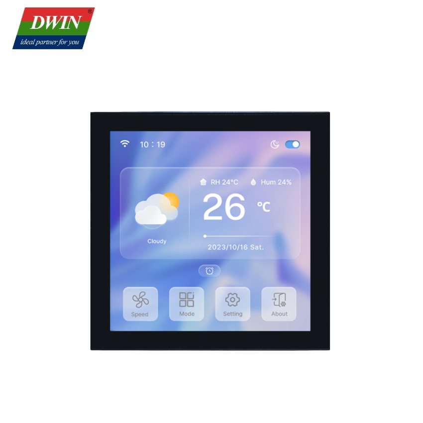

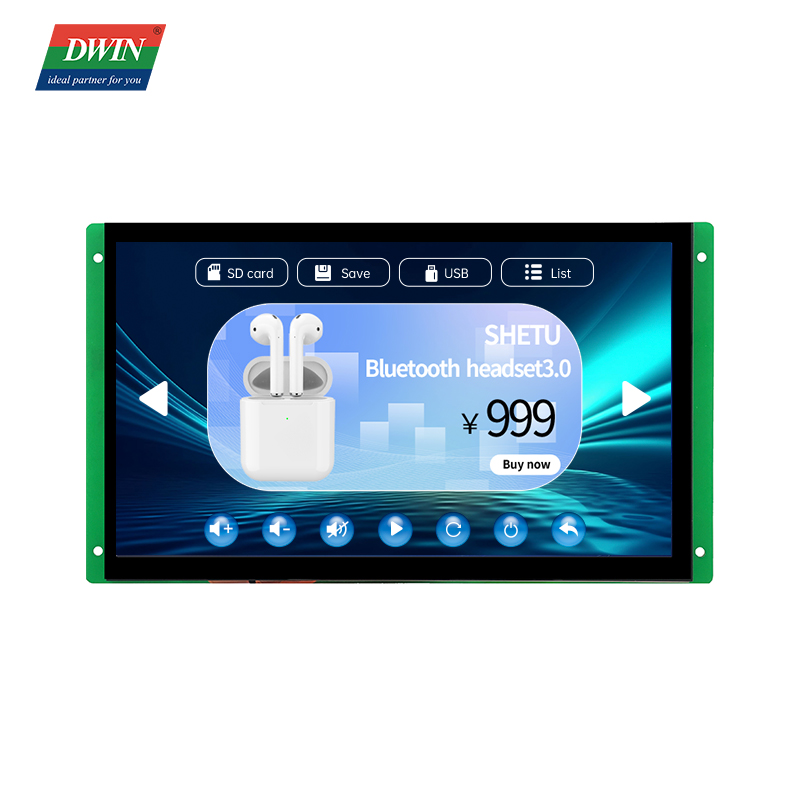
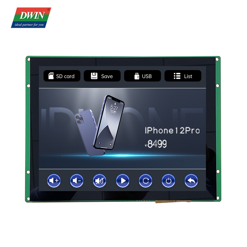
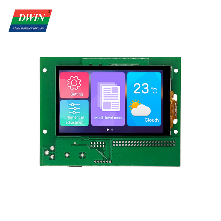
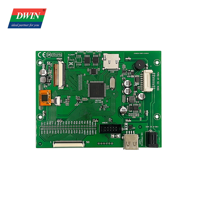
4.0 inch Function Evaluation Touch Panel <br/>Model: EKT040B
Video Specification ASIC Information T5L0 ASIC DWIN seft-design 8051 LCD drive IC. Mass production in 2020, 1MBytes Nor Flash on the chip, 512KBytes used to store the user database. Rewrite cycle: over 100,000 times Display Color 262K(262144)colors LCD Type IPS Viewing Angle 85/85/85/85 (L/R/U/D) Active Area(A.A) 86.00mm (W)×51.44mm (H) Resolution 800X480 Pixel Backlight LED Brightness EKT040B: 250nit; 100 levels adjustment.(It's not recommend to set brightness to 1%~30% of the maximum, which may lead a flicker) LED Lifetime ≥20000H(Continuous working with maximum brightness, time of the brightness decays to 50%) Voltage & Current Power Voltage 6~36V, typical value of 12V Operation Current VCC = +12V, Backlight on,125mA VCC = +12V, Backlight off,55mA Reliability Test Working Temperature -20~70℃(Typical 25℃) Storage Temperature -30~85℃(Typical 25℃) Working Humidity 10%~90%RH Interface Socket 50Pin-0.5mm FCC, 8Pin-2.0mm FCC SD slot YES (SDHC/FAT32 Format) USB Interface YES Peripheral EKT040B Capacitive touch panel, Buzzer Dimension Dimension 119.51mm(W) ×92.25mm(H) ×17.80mm(T) Net Weight 105g Interface Description 1# 8pin-2.0mm FCC power supply interface 2# 6-36V wide voltage power supply interface 3# USB interface, uart1 can be selected 4# SD card burning interface 5# JTAG interface, connected to HME05 emulator or PGT05 burner, used to burn the underlying kernel firmware 6# 2.54mm through hole pad GUI / OS CPU outgoing interface 7# LCD interface 8# Capacitive touch screen interface External Interface PIN Definition Description 1# GND Common ground 2# RX4 UART4 Data reception 3# RX5 UART5 Data reception 4# P01 I / O mouth 5# CRX CAN interface data reception 6# RX2 UART2 data receiving 7# P07 I / O 8# P15 I / O 9# P17 I / O 10# P21 I / O 11# P23 I / O 12# P25 I / O 13# P27 I / O 14# P31 I / O 15# P33 I / O 16# FTX FSK transceiver data reception 17# ADC0 AD input 18# ADC2 AD input 19# ADC5 AD input 20# ADC7 AD input 21# PWM1 16bit PWM output 22# 5V power input 23# TX4 UART4 data transmission 24# TX5 UART5 data transmission 25# P0.0 I / O 26# CTX CAN interface data transmission 27# TX2 UART2 data transmission 28# P06 I / O 29# P14 I / O 30# P16 I / O 31# P20 I / O 32# P22 I / O 33# P24 I / O 34# P26 I / O 35# P30 I / O 36# P32 I / O 37# RSTN System reset input 38# FRX FSK transceiver data transmission 39# ADC1 AD input 40# ADC3 AD input 41# ADC6 AD input 42# PWM0 16bit PWM output