
-
Products
- Video LCD Module
- Touch Panel
- TFT LCD Panel
- TFT LCD Panel
- T5L Evaluation Board
- Switching Power Supply
- LVDS LCD Module
- Linux LCD Module
- IoT Application
- HMI LCD Module
- HDMI LCD Module
- COF UART LCD Module
-
COB UART LCD Module
- 9.7 Inch
- 8.8 Inch
- 8 Inch
- 7.8 Inch
- 7.4 Inch
- 7 Inch
- 6.8 Inch
- 5.7 Inch
- 5.6 Inch
- 5 Inch
- 4.3 Inch
- 4.1 Inch
- 4 Inch
- 32 Inch
- 3.7 Inch
- 3.5 Inch
- 3 Inch
- 27 Inch
- 23.8 Inch
- 21.5 Inch
- 2.8 Inch
- 2.4 Inch
- 2.1 Inch
- 2 Inch
- 18.5 Inch
- 17.3 Inch
- 15.6 Inch
- 15 Inch
- 14 Inch
- 13.3 Inch
- 12.1 Inch
- 11.6 Inch
- 10.4 Inch
- 10.1 Inch
- 1.6 Inch
- 1.54 inch
- 1.3 Inch
- Android LCD Module
- Catalogue

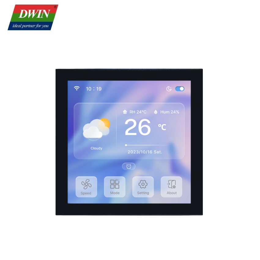
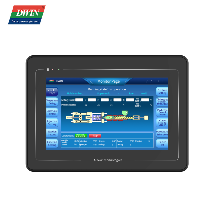

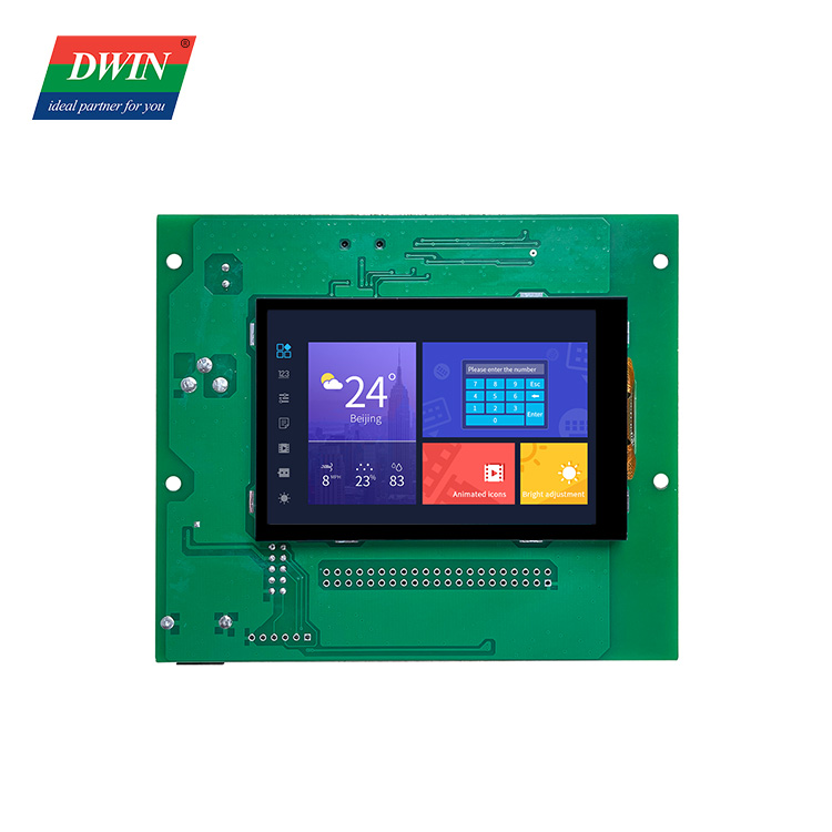
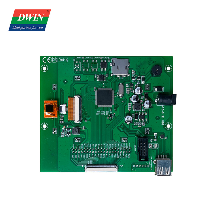
3.5 Inch Function Evaluation Board T5L Model: EKT035B
Video Specification ASIC Information ASIC Information T5L0 ASIC Designed by DWIN. Mass production in 2020, 1MBytes Nor Flash on the chip, 512KBytes used to store the user database. Rewrite cycle: over 100,000 times Display Color 262K(262144)colors LCD Type IPS Viewing Angle 85/85/85/85 (L/R/U/D) Active Area(A.A) 49.0mm (W)×73.4mm (H) Resolution 480X320 Backlight LED Brightness EKT035B: 250nit ;100 levels adjustment.(It's not recommend to set brightness to 1%~30% of the maximum, which may lead a flicker) Voltage & Current Power Voltage 6~36V Operation Current VCC = +12V, Backlight on, 90mA VCC = +12V, Backlight off, 50mA Reliability Test Working Temperature -20~70℃(Typical 25℃) Storage Temperature -30~85℃(Typical 25℃) Working Humidity 10%~90%RH Interface Baudrate 3150~3225600bps Output Voltage Output 1, Iout = 1mA;3.0~3.3 V Output 0, Iout =-1mA;0~0.3 V Input Voltage (RXD) Input 1, Iin = 1mA;2.4~5.0V Input 0, Iin = -1mA;0~0.5V Socket 50Pin-0.5mm FCC, SD Card slot YES (SDHC/FAT32 Format) Peripheral EKT035B Capacitive touch panel, Buzzer Dimension Dimension 105.3mm (W) ×119.5mm(H) ×17.6mm(T) Net Weight 95g Interface Description 1# The FLASH extension module can be used to expand three FLASH modules 2# SD card burning interface 3# Capacitive touch screen interface 4# LCM interface 5# 6-36V wide voltage power supply interface 6# 2.54mm through hole pad GUI / OS CPU outgoing interface 7# JTAG interface, connected to hme05 emulator or pgt05 burner, used to burn the underlying kernel firmware 8# USB interface, UART1 can be selected External Interface PIN Definition Description 1# GND Common ground 2# RX4 UART4 Data reception 3# RX5 UART5 Data reception 4# P01 I / O mouth 5# CRX CAN interface data reception 6# RX2 UART2 data receiving 7# P07 I / O 8# P15 I / O 9# P17 I / O 10# P21 I / O 11# P23 I / O 12# P25 I / O 13# P27 I / O 14# P31 I / O 15# P33 I / O 16# FTX FSK transceiver data reception 17# ADC0 AD input 18# ADC2 AD input 19# ADC5 AD input 20# ADC7 AD input 21# PWM1 16bit PWM output 22# 5V power input 23# TX4 UART4 data transmission 24# TX5 UART5 data transmission 25# P0.0 I / O 26# CTX CAN interface data transmission 27# TX2 UART2 data transmission 28# P06 I / O 29# P14 I / O 30# P16 I / O 31# P20 I / O 32# P22 I / O 33# P24 I / O 34# P26 I / O 35# P30 I / O 36# P32 I / O 37# RSTN System reset input 38# FRX FSK transceiver data transmission 39# ADC1 AD input 40# ADC3 AD input 41# ADC6 AD input 42# PWM0 16bit PWM output Application